Neural Chip Design [4/4: SoC Integration & Firmware]
This is a series of articles [overview] outlining the workflow of 15 steps, which I developed over the past few years through building my own DNN accelerator: Kraken [arXiv paper].
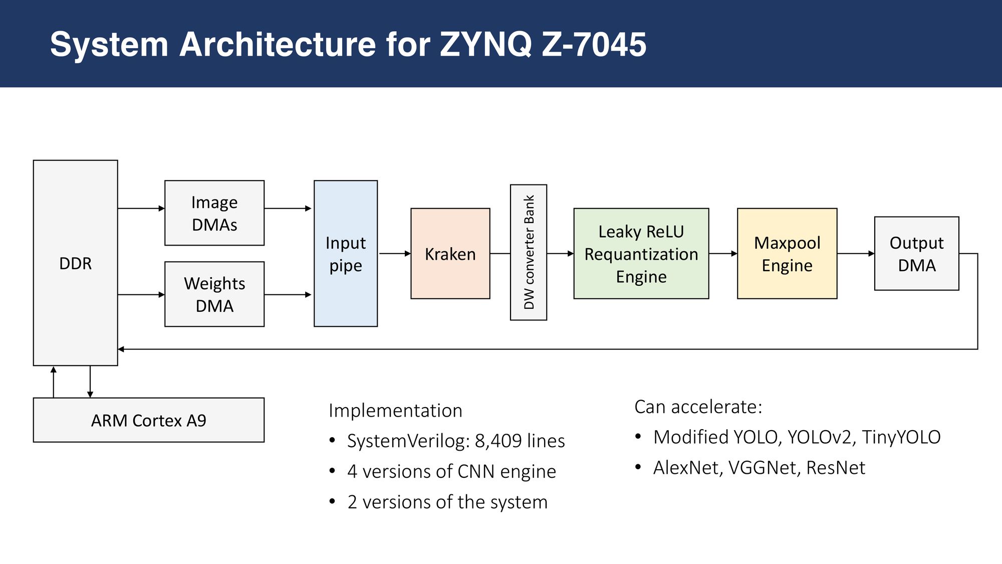
After building and testing each module and combining them hierarchically, it is time to build an SoC around it and control it. I used a Xilinx Zynq Z706 development board with a Z-4045 chip, which has an ARM Cortex processor and a Kintex FPGA on the same silicon die.
The following is the overview of the design. Gray-colored modules are Xilinx IPs. Two soft DMAs pull input \(\hat{X}\) and weight \(\hat{K}\) from the off-chip DDR and feed as two AXI4-Streams, which are then synchronized by the input pipe and provided to the Kraken Engine. The output \(\hat{Y}\) is stored back into the DDR through another soft DMA. The three soft DMAs are controlled by commands issued by the ARM Cortex core, as dictated by the firmware which I then developed.
- SoC Block Design: Build FPGA projects with Vivado manually and synthesize
- Automation: TCL scripts to automate the project building and configuration
- C++ Firmware: To control the custom modules
- Hardware Verification: Test on FPGA, compare output to golden model
- Repeat 11-14
11. SoC Block Design
I add my custom modules to a Vivado block design, add soft DMAs from the IP catalog, configure them, connect them to my main module, run block & connection automation, copying down TCL commands at every step. Below is the final block design I get, first manually, then automating it with TCL scripts.
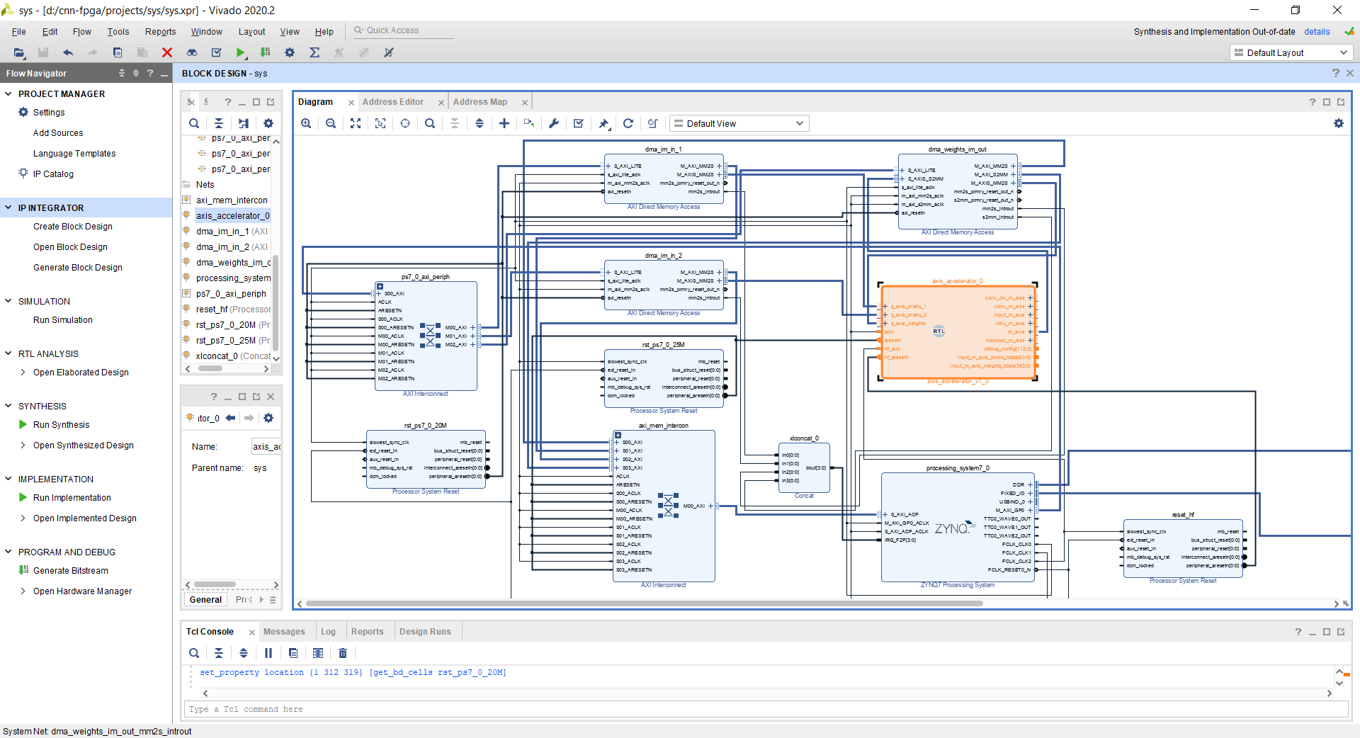
12. TCL Automation
Xilinx Vivado projects are notoriously buggy. They crash once in a while and get corrupted. Vivado also auto-generates hundreds of small files, which contain absolute paths, and don't play well with a different Vivado version. Therefore, it is a bad idea to version control them.
The best practice is to script the project flow. Once I manually copy down the TCL commands, I change them into parameterized code.
set TUSER_WIDTH_MAXPOOL_IN     [expr $BITS_KW2      + $I_KW2]
set TUSER_WIDTH_LRELU_IN       [expr $BITS_KW       + $I_CLR]
set TUSER_CONV_DW_BASE         [expr 1 + $I_IS_BOTTOM_BLOCK ]
set TUSER_CONV_DW_IN           [expr $MEMBERS*$BITS_KW + $BITS_OUT_SHIFT + $BITS_MEMBERS + $TUSER_CONV_DW_BASE]
set TUSER_WIDTH_LRELU_FMA_1_IN [expr 1         + $I_IS_LRELU]
set TUSER_WIDTH_CONV_IN        [expr $I_IS_SUM_START     + 1]

set DEBUG_CONFIG_WIDTH_W_ROT   [expr 1 + 2*$BITS_KW2 + 3*($BITS_KH2      + $BITS_IM_CIN + $BITS_IM_COLS + $BITS_IM_BLOCKS)]
set DEBUG_CONFIG_WIDTH_IM_PIPE [expr 3 + 2 + $BITS_KH2      + 0]
set DEBUG_CONFIG_WIDTH_LRELU   [expr 3 + 4 + $BITS_FMA_2]
set DEBUG_CONFIG_WIDTH_MAXPOOL 1
set DEBUG_CONFIG_WIDTH         [expr $DEBUG_CONFIG_WIDTH_MAXPOOL + $DEBUG_CONFIG_WIDTH_LRELU + 2*$BITS_KH2      + $DEBUG_CONFIG_WIDTH_IM_PIPE + $DEBUG_CONFIG_WIDTH_W_ROT]

# **********    STORE PARAMS    *************
set file_param [open $RTL_DIR/include/params.v w]
if {$MAC_TYPE == "XILINX"} {
  puts $file_param "`define MAC_XILINX 1"
}
if {$REG_TYPE == "ASIC"} {
  puts $file_param "`define ASIC_REG 1"
}
puts $file_param "
`define SRAM_TYPE   \"$SRAM_TYPE\"
`define MAC_TYPE    \"$MAC_TYPE\"
`define UNITS    $UNITS
`define GROUPS   $GROUPS
`define COPIES   $COPIES
`define MEMBERS  $MEMBERS
`define DW_FACTOR_1 $DW_FACTOR_1
`define OUTPUT_MODE \"$OUTPUT_MODE\"
`define KSM_COMBS_EXPR $KSM_COMBS_EXPR
`define KS_COMBS_EXPR $KS_COMBS_EXPRI then spend a couple of days debugging the TCL script to ensure it can reliably rebuild a project from scratch. These TCL scripts and the source Verilog files are tracked by git.
create_bd_design "sys"

# ZYNQ IP
create_bd_cell -type ip -vlnv xilinx.com:ip:processing_system7:5.5 processing_system7_0
apply_bd_automation -rule xilinx.com:bd_rule:processing_system7 -config {make_external "FIXED_IO, DDR" apply_board_preset "1" Master "Disable" Slave "Disable" }  [get_bd_cells processing_system7_0]
set_property -dict [list CONFIG.PCW_FPGA0_PERIPHERAL_FREQMHZ $FREQ_LITE CONFIG.PCW_FPGA1_PERIPHERAL_FREQMHZ $FREQ_LOW CONFIG.PCW_FPGA2_PERIPHERAL_FREQMHZ $FREQ_HIGH CONFIG.PCW_EN_CLK2_PORT $FREQ_LITE CONFIG.PCW_USE_S_AXI_ACP {1} CONFIG.PCW_USE_DEFAULT_ACP_USER_VAL {1} CONFIG.PCW_USE_FABRIC_INTERRUPT {1} CONFIG.PCW_EN_CLK1_PORT {1} CONFIG.PCW_EN_CLK2_PORT {1} CONFIG.PCW_IRQ_F2P_INTR {1} CONFIG.PCW_QSPI_PERIPHERAL_ENABLE {0} CONFIG.PCW_SD0_PERIPHERAL_ENABLE {0} CONFIG.PCW_I2C0_PERIPHERAL_ENABLE {0} CONFIG.PCW_GPIO_MIO_GPIO_ENABLE {0}] [get_bd_cells processing_system7_0]

# Accelerator
create_bd_cell -type module -reference axis_accelerator axis_accelerator_0

# Weights & out DMA
set IP_NAME "dma_weights_im_out"
create_bd_cell -type ip -vlnv xilinx.com:ip:axi_dma:7.1 $IP_NAME
set_property -dict [list CONFIG.c_include_sg {0} CONFIG.c_sg_length_width {26} CONFIG.c_m_axi_mm2s_data_width {32} CONFIG.c_m_axis_mm2s_tdata_width {32} CONFIG.c_mm2s_burst_size {8} CONFIG.c_sg_include_stscntrl_strm {0} CONFIG.c_include_mm2s_dre {1} CONFIG.c_m_axi_mm2s_data_width $S_WEIGHTS_WIDTH_LF CONFIG.c_m_axis_mm2s_tdata_width $S_WEIGHTS_WIDTH_LF CONFIG.c_m_axi_s2mm_data_width $M_DATA_WIDTH_LF CONFIG.c_s_axis_s2mm_tdata_width $M_DATA_WIDTH_LF CONFIG.c_include_s2mm_dre {1} CONFIG.c_s2mm_burst_size {16}] [get_bd_cells $IP_NAME]

# Im_in_1
set IP_NAME "dma_im_in"
create_bd_cell -type ip -vlnv xilinx.com:ip:axi_dma:7.1 $IP_NAME
set_property -dict [list CONFIG.c_include_sg {0} CONFIG.c_sg_length_width {26} CONFIG.c_m_axi_mm2s_data_width [expr $S_PIXELS_WIDTH_LF] CONFIG.c_m_axis_mm2s_tdata_width [expr $S_PIXELS_WIDTH_LF] CONFIG.c_include_mm2s_dre {1} CONFIG.c_mm2s_burst_size {64} CONFIG.c_include_s2mm {0}] [get_bd_cells $IP_NAME]

# # Interrupts
create_bd_cell -type ip -vlnv xilinx.com:ip:xlconcat:2.1 xlconcat_0
set_property -dict [list CONFIG.NUM_PORTS {4}] [get_bd_cells xlconcat_0]
connect_bd_net [get_bd_pins dma_im_in/mm2s_introut] [get_bd_pins xlconcat_0/In0]
connect_bd_net [get_bd_pins dma_weights_im_out/mm2s_introut] [get_bd_pins xlconcat_0/In2]
connect_bd_net [get_bd_pins dma_weights_im_out/s2mm_introut] [get_bd_pins xlconcat_0/In3]
connect_bd_net [get_bd_pins xlconcat_0/dout] [get_bd_pins processing_system7_0/IRQ_F2P]

# Engine connections
connect_bd_net [get_bd_pins processing_system7_0/FCLK_CLK1] [get_bd_pins axis_accelerator_0/aclk]
connect_bd_net [get_bd_pins processing_system7_0/FCLK_CLK2] [get_bd_pins axis_accelerator_0/hf_aclk]
connect_bd_intf_net [get_bd_intf_pins dma_im_in/M_AXIS_MM2S] [get_bd_intf_pins axis_accelerator_0/s_axis_pixels]
connect_bd_intf_net [get_bd_intf_pins dma_weights_im_out/M_AXIS_MM2S] [get_bd_intf_pins axis_accelerator_0/s_axis_weights]
switch $OUTPUT_MODE {
  "CONV"    {connect_bd_intf_net [get_bd_intf_pins dma_weights_im_out/S_AXIS_S2MM] [get_bd_intf_pins axis_accelerator_0/conv_dw2_lf_m_axis]}
  "LRELU"   {connect_bd_intf_net [get_bd_intf_pins dma_weights_im_out/S_AXIS_S2MM] [get_bd_intf_pins axis_accelerator_0/lrelu_dw_lf_m_axis]}
  "MAXPOOL" {connect_bd_intf_net [get_bd_intf_pins dma_weights_im_out/S_AXIS_S2MM] [get_bd_intf_pins axis_accelerator_0/max_dw2_lf_m_axis ]}
}

# AXI Lite
startgroup
apply_bd_automation -rule xilinx.com:bd_rule:axi4 -config { Clk_master {/processing_system7_0/FCLK_CLK0 ($FREQ_LITE MHz)} Clk_slave {/processing_system7_0/FCLK_CLK0 ($FREQ_LITE MHz)} Clk_xbar {/processing_system7_0/FCLK_CLK0 ($FREQ_LITE MHz)} Master {/processing_system7_0/M_AXI_GP0} Slave {/dma_im_in/S_AXI_LITE} ddr_seg {Auto} intc_ip {New AXI Interconnect} master_apm {0}}  [get_bd_intf_pins dma_im_in/S_AXI_LITE]
apply_bd_automation -rule xilinx.com:bd_rule:axi4 -config { Clk_master {/processing_system7_0/FCLK_CLK0 ($FREQ_LITE MHz)} Clk_slave {/processing_system7_0/FCLK_CLK0 ($FREQ_LITE MHz)} Clk_xbar {/processing_system7_0/FCLK_CLK0 ($FREQ_LITE MHz)} Master {/processing_system7_0/M_AXI_GP0} Slave {/dma_weights_im_out/S_AXI_LITE} ddr_seg {Auto} intc_ip {New AXI Interconnect} master_apm {0}}  [get_bd_intf_pins dma_weights_im_out/S_AXI_LITE]
endgroup

# AXI4
startgroup
apply_bd_automation -rule xilinx.com:bd_rule:axi4 -config { Clk_master {/processing_system7_0/FCLK_CLK1 ($FREQ_LOW MHz)} Clk_slave {/processing_system7_0/FCLK_CLK1 ($FREQ_LOW MHz)} Clk_xbar {/processing_system7_0/FCLK_CLK1 ($FREQ_LOW MHz)} Master {/dma_weights_im_out/M_AXI_MM2S} Slave {/processing_system7_0/S_AXI_ACP} ddr_seg {Auto} intc_ip {New AXI Interconnect} master_apm {0}}  [get_bd_intf_pins processing_system7_0/S_AXI_ACP]
apply_bd_automation -rule xilinx.com:bd_rule:axi4 -config { Clk_master {/processing_system7_0/FCLK_CLK1 ($FREQ_LOW MHz)} Clk_slave {/processing_system7_0/FCLK_CLK1 ($FREQ_LOW MHz)} Clk_xbar {/processing_system7_0/FCLK_CLK1 ($FREQ_LOW MHz)} Master {/dma_im_in/M_AXI_MM2S} Slave {/processing_system7_0/S_AXI_ACP} ddr_seg {Auto} intc_ip {/axi_mem_intercon} master_apm {0}}  [get_bd_intf_pins dma_im_in/M_AXI_MM2S]
apply_bd_automation -rule xilinx.com:bd_rule:axi4 -config { Clk_master {/processing_system7_0/FCLK_CLK1 ($FREQ_LOW MHz)} Clk_slave {/processing_system7_0/FCLK_CLK1 ($FREQ_LOW MHz)} Clk_xbar {/processing_system7_0/FCLK_CLK1 ($FREQ_LOW MHz)} Master {/dma_weights_im_out/M_AXI_S2MM} Slave {/processing_system7_0/S_AXI_ACP} ddr_seg {Auto} intc_ip {/axi_mem_intercon} master_apm {0}}  [get_bd_intf_pins dma_weights_im_out/M_AXI_S2MM]
endgroup

# HF Reset
set IP_NAME "reset_hf"
create_bd_cell -type ip -vlnv xilinx.com:ip:proc_sys_reset:5.0 $IP_NAME
connect_bd_net [get_bd_pins processing_system7_0/FCLK_CLK2] [get_bd_pins $IP_NAME/slowest_sync_clk]
connect_bd_net [get_bd_pins processing_system7_0/FCLK_RESET0_N] [get_bd_pins $IP_NAME/ext_reset_in]
connect_bd_net [get_bd_pins $IP_NAME/peripheral_aresetn] [get_bd_pins axis_accelerator_0/hf_aresetn]

# LF Reset
# NOTE: axi_mem_intercon gets created after axi lite
connect_bd_net [get_bd_pins axis_accelerator_0/aresetn] [get_bd_pins axi_mem_intercon/ARESETN]

save_bd_design
validate_bd_design

generate_target all [get_files  $PROJ_FOLDER/$PROJ_NAME.srcs/sources_1/bd/sys/sys.bd]
make_wrapper -files [get_files $PROJ_FOLDER/$PROJ_NAME.srcs/sources_1/bd/sys/sys.bd] -top
add_files -norecurse $PROJ_FOLDER/$PROJ_NAME.gen/sources_1/bd/sys/hdl/sys_wrapper.v
set_property top sys_wrapper [current_fileset]13. C++ Firmware
I then write the C++ code to be run on the ARM processor, which instructs the DMA to pull data from memory and push it back. When multiple DMAs are involved, this is fairly tricky. Right after starting a DMA operation, the parameters for the next DMA iteration must be calculated in advance, to prevent stalling the DMA.
13.1. OOP Wrappers for DMA Drivers
I find the C code provided by Xilinx a bit counterintuitive. Therefore, I have written an OOP wrapper for the Xilinx DMA, which is open-sourced here:
 abarajithan11
13.2. OOP Architecture for DNN models & config bits in C++
The firmware needs to be flexible, such that I can create any DNN by chaining layer objects. For this, I write the layer class, with necessary features like extracting configuration bits and appending to data.
class Layer
{
public:
	 int idx, H_IN, W_IN, C_IN, C_OUT, KH_IN, KW_IN;
	 bool IS_NOT_MAX, IS_MAX, IS_LRELU;

	 Layer * PREV_P = nullptr;
	 Layer * NEXT_P = nullptr;

	 int BLOCKS, BLOCKS_PER_ARR;
	 u8 MAX_FACTOR, SUB_CORES, EFF_CORES, ITR, COUT_FPGA, COUT_VALID, COUT_INVALID;
	 u8 KW_PAD;

	 int OUT_W_IN, OUT_BLOCKS, OUT_MAX_FACTOR, OUT_BLOCKS_PER_ARR, OUT_KH;

	 int DATA_BEATS_PIXELS;
	 int BEATS_LRELU = 0;
	 int WORDS_PIXELS_PER_ARR;
	 int WORDS_WEIGHTS_PER_ITR, WORDS_WEIGHTS;

	 int WORDS_OUT_PER_TRANSFER, TRANSFERS_OUT_PER_ITR;
	 int WORDS_OUT_PER_TRANSFER_ARR [3];

	 chunk_s * input_chunk_p  = nullptr;
	 chunk_s * output_chunk_p = nullptr;
	 bool done_write = false;

	 Layer ( int idx,
			 int H_IN, int W_IN, int C_IN, int C_OUT,
			 int KH_IN, int KW_IN,
			 bool IS_NOT_MAX, bool IS_MAX, bool IS_LRELU):
					 idx    (idx),
					 H_IN   (H_IN),
					 W_IN   (W_IN),
					 C_IN   (C_IN),
					 C_OUT  (C_OUT),
					 KH_IN   (KH_IN),
					 KW_IN   (KW_IN),
					 IS_NOT_MAX(IS_NOT_MAX),
					 IS_MAX    (IS_MAX),
					 IS_LRELU  (IS_LRELU)
	 {
		 BLOCKS     = H_IN / UNITS;
		 MAX_FACTOR = IS_MAX ? 2 : 1;
		 BLOCKS_PER_ARR = BLOCKS / MAX_FACTOR;

		 KW_PAD = KW_IN - 2*IS_MAX;

		 SUB_CORES = MEMBERS / KW_IN;
		 EFF_CORES = COPIES * GROUPS * SUB_CORES / MAX_FACTOR;
		 ITR       = (int)(std::ceil((float)C_OUT / (float)EFF_CORES));
		 COUT_FPGA = EFF_CORES * ITR;

		 COUT_VALID = C_OUT % EFF_CORES;
		 COUT_VALID = (COUT_VALID == 0) ? EFF_CORES : COUT_VALID;

		 COUT_INVALID = EFF_CORES - COUT_VALID;

		 /* LRELU BEATS */

		 BEATS_LRELU += 1; //D
		 BEATS_LRELU += ceil(2.0/KW_IN); // A

		 for (int clr_i=0;  clr_i < KW_IN/2+1; clr_i ++){
			 int clr = clr_i*2 +1;
			 for (int mtb=0;  mtb < clr; mtb ++){
				 int bram_width = MEMBERS/clr;
				 int bram_size  = 2*SUB_CORES;
				 int BEATS_ij = ceil((float)bram_size/bram_width);

				 BEATS_LRELU += BEATS_ij;
			 }
		 }

		 DATA_BEATS_PIXELS = BLOCKS_PER_ARR * W_IN * C_IN;

		 WORDS_PIXELS_PER_ARR  =      DATA_BEATS_PIXELS  * UNITS_EDGES;
		 WORDS_WEIGHTS_PER_ITR = (S_WEIGHTS_WIDTH/8) + (BEATS_LRELU + C_IN*KH_IN) * COPIES * GROUPS * MEMBERS;
		 WORDS_WEIGHTS         = ITR * WORDS_WEIGHTS_PER_ITR;

		 if (IS_NOT_MAX && IS_MAX)
		 {
			 WORDS_OUT_PER_TRANSFER_ARR[0] = SUB_CORES * COPIES * GROUPS * UNITS_EDGES;
			 WORDS_OUT_PER_TRANSFER_ARR[1] =             COPIES * GROUPS * UNITS_EDGES;
			 WORDS_OUT_PER_TRANSFER_ARR[2] =             COPIES * GROUPS * UNITS_EDGES / MAX_FACTOR;

			 TRANSFERS_OUT_PER_ITR = BLOCKS/MAX_FACTOR * W_IN/MAX_FACTOR * (1 + 2 * SUB_CORES);
		 }
		 else
		 {
			 WORDS_OUT_PER_TRANSFER = SUB_CORES * COPIES * GROUPS * UNITS_EDGES / MAX_FACTOR;
			 TRANSFERS_OUT_PER_ITR  = BLOCKS/MAX_FACTOR * W_IN/MAX_FACTOR;
		 }
	 };

	 void set_config()
	 {
		 input_chunk_p->data_p[0] = (s8)(IS_NOT_MAX);
		 input_chunk_p->data_p[1] = (s8)(IS_MAX);
		 input_chunk_p->data_p[2] = (s8)(IS_LRELU);
		 input_chunk_p->data_p[3] = (s8)(KH_IN/2);

#ifdef DEBUG
		 for (int i=4; i<UNITS_EDGES; i++) input_chunk_p->data_p[i] = 0;
#endif
		 Xil_DCacheFlushRange((UINTPTR)input_chunk_p->data_p, UNITS_EDGES);
	 };

	 void set_out_params()
	 {
		 /* Next layer can be null (if this is last) or can have multiple next layers.
		  * We are interested in how to arrange the output values of this, to match the next
		  */

		 OUT_W_IN   = W_IN / MAX_FACTOR;
		 OUT_BLOCKS = (H_IN / MAX_FACTOR) / UNITS;

		 OUT_MAX_FACTOR     = (NEXT_P == nullptr) ? 1 : NEXT_P->MAX_FACTOR;
		 OUT_BLOCKS_PER_ARR = OUT_BLOCKS/OUT_MAX_FACTOR;

		 OUT_KH = (NEXT_P == nullptr) ? KH_IN : NEXT_P->KH_IN;
	 }

	 inline s8* get_input_pixels_base_p()
	 {
		 return (s8*)(input_chunk_p->data_p) + UNITS_EDGES;
	 }
	 inline s8* get_output_pixels_base_p()
	 {
		 return (s8*)(output_chunk_p->data_p) + UNITS_EDGES;
	 }
};
auto build_yolo_mod()
{
std::array<Layer,21> layers = {
Layer(1, H_RGB ,W_RGB , 3, 32, 3, 3,false, true, true),
Layer(2, H_RGB/2 ,W_RGB/2, 32, 64, 3, 3,false, true, true),
Layer(3, H_RGB/4 ,W_RGB/4, 64, 128, 3, 3,true, false, true),
Layer(4, H_RGB/4 ,W_RGB/4, 128, 64, 1, 1,true, false, true),
Layer(5, H_RGB/4 ,W_RGB/4, 64, 128, 3, 3,false, true, true),
Layer(6, H_RGB/8 ,W_RGB/8, 128, 256, 3, 3,true, false, true),
Layer(7, H_RGB/8 ,W_RGB/8, 256, 128, 1, 1,true, false, true),
Layer(8, H_RGB/8 ,W_RGB/8, 128, 256, 3, 3,false, true, true),
Layer(9, H_RGB/16,W_RGB/16, 256, 512, 3, 3,true, false, true),
Layer(10, H_RGB/16,W_RGB/16, 512, 256, 1, 1,true, false, true),
Layer(11, H_RGB/16,W_RGB/16, 256, 512, 3, 3,true, false, true),
Layer(12, H_RGB/16,W_RGB/16, 512, 256, 1, 1,true, false, true),
Layer(13, H_RGB/16,W_RGB/16, 256, 512, 3, 3,false, true, true),
Layer(14, H_RGB/32,W_RGB/32, 512,1024, 3, 3,true, false, true),
Layer(15, H_RGB/32,W_RGB/32,1024, 512, 1, 1,true, false, true),
Layer(16, H_RGB/32,W_RGB/32, 512,1024, 3, 3,true, false, true),
Layer(17, H_RGB/32,W_RGB/32, 64, 128,1024, 512,true, false, true),
Layer(18, H_RGB/32,W_RGB/32, 64, 128, 512,1024,true, false, true),
Layer(19, H_RGB/32,W_RGB/32,1024,1024, 3, 3,true, false, true),
Layer(20, H_RGB/32,W_RGB/32,1024,1024, 3, 3,true, false, true),
Layer(21, H_RGB/32,W_RGB/32,1024, 45, 1, 1,true, false, false)
};
for (int i=0; i < N_LAYERS; i++)
{
if (i!=0 ) layers[i].PREV_P = &layers[i-1];
if (i!=N_LAYERS-1) layers[i].NEXT_P = &layers[i+1];
layers[i].set_out_params();
}
return layers;
}13.3. C++ Code to control multiple DMAs effectively
Next, I write C++ functions to reshape the output (\hat{Y}\) on the fly (after each small DMA packet) to generate the next layers input \(\hat{X}\). Also, configuration bits need to be calculated and appended to the packet to make it complete.
void restart_output()
{
	static int i_w=0, i_w_flipped=0, i_blocks=0, i_bpa=0, i_arr=0, i_cout=0, i_itr=0, i_layers=i_layers_start;
	static volatile s8 * write_p = layers[i_layers].get_output_pixels_base_p();
	static bool is_new_layer=true;

    static volatile s8 * write_p_old = 0;
	Xil_DCacheFlushRange((UINTPTR)write_p_old, UNITS_EDGES);

	if ((i_itr == 0 && i_blocks == 31) || (i_itr == 1 && i_blocks == 0)){
		for (int i=0; i<UNITS_EDGES; i++){
			PRINT(" %d,", write_p_old[i]);
		}
		PRINT("] \r\n");
		PRINT("(%d,%d,%d,%d-%d,:) -- %p [", i_arr, i_bpa, i_w_flipped,i_itr,i_cout, write_p);
	}
	write_p_old = write_p;

	// start transfer
	dma_weights_im_out.s2mm_start(	(UINTPTR)write_p,
									layers[i_layers].WORDS_OUT_PER_TRANSFER);

	pad_prev(i_w_flipped,i_blocks,i_bpa,i_arr,i_cout,i_layers);

	// set config
	if (is_new_layer && i_layers != N_LAYERS-1)
	{
		layers[i_layers].NEXT_P->set_config();
		layers[i_layers].NEXT_P->done_write = false;
		is_new_layer = false;
	}

	// PREPARE NEXT INDICES
	// blocks = 31 (a=1,bpa=15), w_f = 191 (w = 190), itr = 0
	if (i_w < layers[i_layers].OUT_W_IN-1)
	{
		i_w += 1;
		// Flip last KW-1 columns : flipped = 2w-(kw+iw)
		// For max: kw <- kw-2
		if (i_w > layers[i_layers].OUT_W_IN - layers[i_layers].KW_PAD)
			i_w_flipped = 2 * layers[i_layers].OUT_W_IN - (i_w + layers[i_layers].KW_PAD);
		else
			i_w_flipped = i_w;
	}
	else
	{
		i_w = 0;
		i_w_flipped = 0;

		 PRINT(" i_blocks: %d, write_p: %p \r\n", i_blocks, write_p);

		if (i_blocks < layers[i_layers].OUT_BLOCKS-1)
		{
			i_blocks  += 1;
			i_arr      = i_blocks % layers[i_layers].OUT_MAX_FACTOR;
			i_bpa      = i_blocks / layers[i_layers].OUT_MAX_FACTOR;
		}
		else
		{
			i_blocks   = 0;
			i_arr      = 0;
			i_bpa      = 0;

			 PRINT(" i_itr: %d \r\n", i_itr);

			if (i_itr >= layers[i_layers].ITR-1)
			{
				is_new_layer = true;
				i_itr = 0;
				i_cout= 0;

				if (i_layers < N_LAYERS-1)
					i_layers += 1;
				else
				{
					i_layers = 0;
					done = true;
					PRINT("All Layers done \r\n");
				}

				/* Chaining*/
				if (i_layers == N_LAYERS-1)
				{
					layers[0].input_chunk_p = &temp_in_chunk;
					layers[i_layers].output_chunk_p = &temp_out_chunk;
				}
				else
				{
					layers[i_layers].output_chunk_p = get_chunk();
					layers[i_layers].NEXT_P->input_chunk_p = layers[i_layers].output_chunk_p;
				}
				PRINT("Writing to new layer: chained_chunks (idx:%d -> idx:%d), data_p= %p \r\n",
						    layers[i_layers].idx, layers[i_layers].NEXT_P->idx,
							layers[i_layers].output_chunk_p->data_p);

				layers[i_layers].print_output_params();
			}
			else if (i_itr == 0)
			{
				i_itr += 1;
				i_cout = layers[i_layers].COUT_VALID;
			}
			else
			{
				i_itr  += 1;
				i_cout += layers[i_layers].EFF_CORES;
			}
		}
	}
	// blocks = 31 (a=1,bpa=15), w_f = 191, itr = 0
	write_p = unravel_image_abwcu(layers[i_layers].get_output_pixels_base_p(),
								  i_arr,i_bpa,i_w_flipped,i_cout,0, i_layers);
}
14. Hardware (FPGA) Verification
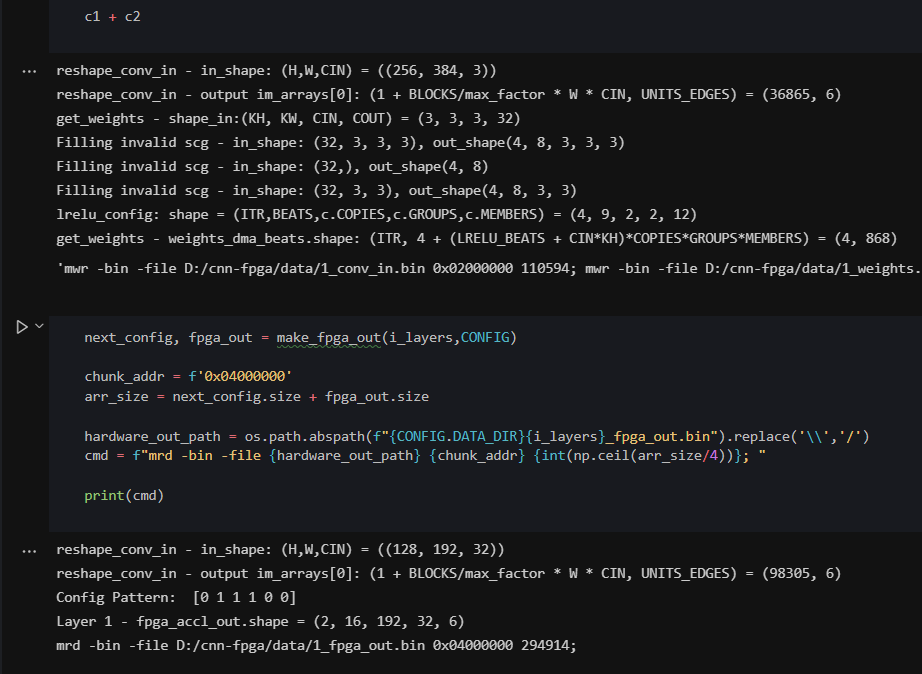
15. Repeat 11-14
I spent weeks or months repeating 11-14, to finally get the hardware outputs to match the golden model, and hence the original DNNs. Once I spent a month figuring out a bug where the system worked perfectly in randomized simulations but had wrong values for just 6 bytes out of 4 million bytes. Finally, I found it's a bug in Vivado's compiler.